For professionals within Electronics, a digital microscope is an excellent tool for soldering and PCB inspections.
With 60 frames per second, you’ll experience a smooth live image as you’re moving the PCB around to spot issues during your production. Any findings can easily be documented, stored or forwarded to business partners to discuss how to proceed.
The digital display also makes it easy to ask a colleague for a second opinion or train new employees as you’re able to look at a sample together rather than taking turns looking through the ocular of a traditional microscope.
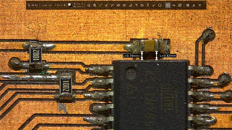
With a digital microscope from TAGARNO, you can also activate apps that’ll assist you in securing the quality of the PCBs while also increasing your efficiency. This includes Measurement app, Focus stacking app, Image comparison app and DXF overlay app.
Below, we’ll go into more detail with how a digital microscope and which apps can be used for different processes within Electronics.
Research and development
The high image quality and easy documentation process of a digital microscope makes it the perfect inspection tool when the goal is to create as much documentation as possible – especially for First article inspections (FAI).
Add-on software such as Measurement app, Focus stacking app and DXF overlay app are also beneficial in documenting that each component has been placed as specified.
Here’s the microscope we recommend for FAI
Quality assurance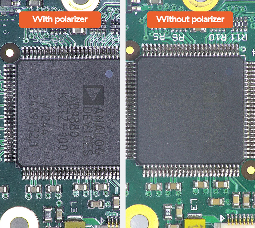
The high image quality and smooth live image of TAGARNO’s digital microscopes makes it easy to check if components have been placed correctly during production. With apps like Image comparison, you can even compare your current PCB to a photo of a golden sample to quickly spot deviations.
Studies show that introducing simple ergonomic improvements to processes like this can reduce PCB escape rates and ultimately reduce customer claims.